
ESD Solutions
General-Purpose I/O (GPIO)
Aragio’s wide portfolio of general-purpose I/Os is targeted to meet the critical performance, power, area and reliability (ESD and latch-up tolerance) requirements for IC designs. These general-purpose I/O circuits include a full set of power pads, corner pad cells, breakers and spacers. These designs are implemented with special design considerations for power supply sequencing requirements. Distributed Power-on-Control (POC) is used during power up and power down of the systems.
GPIO: 1.2V-1.5V-1.8V
Summary
A full range of power pads is provided to enable the system designer different options for separate core power (VDD and VSS) and separate I/O padring power and ground (DVDD and DVSS). The ability to isolate separate power domains is also provided. In addition, the I/O library has a full complement of cells that provide the user with the ability to isolate analog I/O’s and power within the same padring as the digital I/O’s.
Includes:
- Programmable GPIO
- Programmable fault-tolerant GPIO
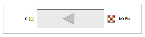
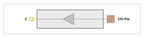
- Input buffer
- Power supplies
- Isolated analog power supplies
- Full complement of support pads
Diagram (driver)
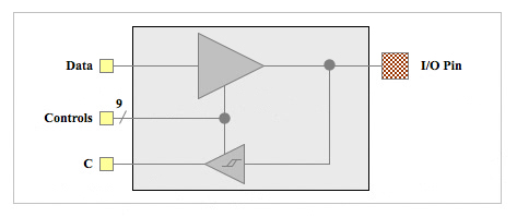
Diagram (input)
Recommended Operating Conditions
| Description | Min | Nom | Max | Units | |
|---|---|---|---|---|---|
| VDVDD | I/O supply voltage | 1.08 | 1.2 | 1.32 | V |
| 1.35 | 1.5 | 1.65 | V | ||
| 1.62 | 1.8 | 1.98 | V | ||
| TA | Ambient operating temperature | 0 | 25 | 100 | °C |
| VVDD | Core supply voltage | 0.9 | 1.0 to 1.1 | 1.155 | V |
| TJ | Junction temperature | -40 | 25 | 125 | °C |
| VPAD | Voltage at PAD | 0 | - | VDVDD | V |
| VIH | Input logic high | 0.7 * VDVDD | VDVDD + 0.3 | V | |
| VIL | Input logic low | VDVSS – 0.3 | 0.3 * VDVDD | V |
Foundry Support
| Technology | Silicon proven / in production | Under development | Planned |
|---|---|---|---|
| 07nm | TSMC | ||
| 12nm | TSMC | ||
| 16nm | GF, TSMC | ||
| 22nm | GF | ||
| 28nm | GF, TSMC | ||
| 40nm | GF | ||
| 55nm | |||
| 65nm | |||
| 90nm | |||
| 110nm | |||
| 130nm |
GPIO: 1.5V-1.8V-2.5V
Summary
A full range of power pads is provided to enable the system designer different options for separate core power (VDD and VSS) and separate I/O padring power and ground (DVDD and DVSS). The ability to isolate separate power domains is also provided. In addition, the I/O library has a full complement of cells that provide the user with the ability to isolate analog I/O’s and power within the same padring as the digital I/O’s.
Includes:
- Programmable GPIO
- Programmable fault-tolerant GPIO
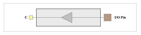
- Input buffer
- Power supplies
- Isolated analog power supplies
- Oscillators
- Full complement of support pads
Diagram (driver)
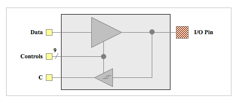
Diagram (input)
Recommended Operating Conditions
| Description | Min | Nom | Max | Units | |
|---|---|---|---|---|---|
| VDVDD | I/O supply voltage | 1.35 | 1.5 | 1.65 | V |
| 1.62 | 1.8 | 1.98 | V | ||
| 2.25 | 2.5 | 2.75 | V | ||
| TA | Ambient operating temperature | 0 | 25 | 100 | °C |
| VVDD | Core supply voltage | 0.9 | 1.0 to 1.1 | 1.155 | V |
| TJ | Junction temperature | -40 | 25 | 125 | °C |
| VPAD | Voltage at PAD | 0 | - | VDVDD | V |
| VIH | Input logic high | 0.7 * VDVDD | VDVDD + 0.3 | V | |
| VIL | Input logic low | VDVSS – 0.3 | 0.3 * VDVDD | V |
Foundry Support
| Technology | Silicon proven / in production | Under development | Planned |
|---|---|---|---|
| 28nm | GF | ||
| 40nm | TSMC, SMIC | ||
| 55nm | GF | ||
| 65nm | GF | ||
| 90nm | |||
| 110nm | |||
| 130nm |
GPIO: 1.8V-2.5V-2.8V-3.0V-3.3V
Summary
A full range of power pads is provided to enable the system designer different options for separate core power (VDD and VSS) and separate I/O padring power and ground (DVDD and DVSS). The ability to isolate separate power domains is also provided. In addition, the I/O library has a full complement of cells that provide the user with the ability to isolate analog I/O’s and power within the same padring as the digital I/O’s.
Includes
- Programmable GPIO
- Programmable fault-tolerant GPIO
- Input buffer
- Power supplies
- Isolated analog power supplies
- Programmable oscillator
- Full complement of support pads
Diagram (GPIO)
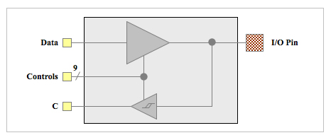
Diagram (input)
Recommended Operating Conditions
| Description | Min | Nom | Max | Units | |
|---|---|---|---|---|---|
| VDVDD | I/O supply voltage | 2.97 | 3.3 | 3.63 | V |
| 2.70 | 3.0 | 3.30 | V | ||
| 2.52 | 2.8 | 3.08 | V | ||
| 2.25 | 2.5 | 2.50 | V | ||
| 1.62 | 1.8 | 1.98 | V | ||
| 1.08 | 1.2 | 1.32 | V | ||
| TA | Ambient operating temperature | 0 | 25 | 100 | °C |
| VVDD | Core supply voltage | 0.9 | 0.8v to 1.2 | 1.32 | V |
| TJ | Junction temperature | -40 | 25 | 125 | °C |
| VPAD | Voltage at PAD | 0 | - | VDVDD | V |
| VIH | Input logic high | 0.7 * VDVDD | VDVDD + 0.3 | V | |
| VIL | Input logic low | VDVSS – 0.3 | 0.3 * VDVDD | V |
Foundry Support
| Technology | Silicon proven / in production | Under development |
|---|---|---|
| 7nm | TSMC | |
| 12nm | TSMC | |
| 16nm | TSMC | |
| 22nm | GF | |
| 28nm | GF, TSMC | |
| 40nm | GF, TSMC, SMIC | |
| 55nm | GF | |
| 65nm | GF, TSMC | |
| 90nm | GF | |
| 110nm | GF | |
| 130nm | GF |